2022-11-29
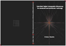
Dark-Field Digital Holographic Microscopy For Advanced Semiconductor Metrology
Publication
Publication
The goal of this thesis is to investigate the potential use of dark-field Digital Holographic Microscopy for advanced semiconductor overlay metrology. We will present first overlay metrology results using a novel off-axis dark-field digital holographic microscopy concept that acquires multiple holograms in parallel by angular frequency multiplexing. The presented results show potential for significant improvement and that digital holographic microscopy is a promising technique for future overlay metrology tools. Theoretical analysis and experimental investigations will be presented to validate this potential and quantify to which extent it can be considered the future overlay metrology tool. This thesis also includes a brief introduction to semiconductor industry and the challenges of semiconductor metrology and clarifies the context of our research towards the use of holographic microscopy with an overview of holography and its application.
| Additional Metadata | |
|---|---|
| A.J. den Boef (Arie) , S. Witte (Stefan) , J.F. de Boer (Johannes) | |
| VU University Amsterdam | |
| Organisation | Computational Imaging |
|
Messinis, C. (2022, November 29). Dark-Field Digital Holographic Microscopy For Advanced Semiconductor Metrology. |
|

